Table of Content
It does make me wonder how it might be possible to modify other photoresist application methods to accommodate this process. I really like the laser printer based photoresist method since it’s so precise. On the other hand, you can use homemade PCBs for prototypes and replace defective PCBs that you can't find on the market. In this case, ordering 1000 PCBs for fixing your Grandpa's old radio doesn't make sense. In addition, the copper foil is much thinner than the layer of copper you use in DIY projects. The thickness of a 2 layer PCB is typically around 3.2 mm, but can range from 2.8 mm to 4.0 mm.
It has higher assembly density than single-layer and double-layer PCBs. Peel off the remaining dry film, leaving only the remaining copper pattern as the inner layer. However, 4 to 8 layers PCBs are commonly used in various applications. The circuit becomes complicated when the number of layers increases. So you can customize it according to your own needs and different layers.
Checking if the site connection is secure
Multilayer PCBs are inherently light-weight & easy to work within complex machinery & yields higher mobility. Make sure to test your PCB before using it in your project. This will ensure that it is working properly and that there are no defects. The width of the traces on your PCB will also affect its performance.

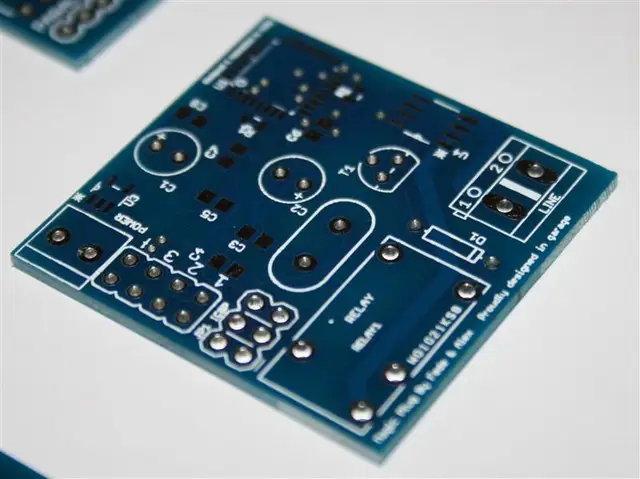
Make sure that the design is correct with proper placement of the components. A Multilayer PCB is a class of PCB that consists of 2, 3, or more conductive copper foil layers. It generally appears as many layers of a double-sided circuit board, laminated and glued together with various layers of heat-protective insulation between them. A conductive pathway is etched on both sides for connecting different components. All circuit connections among the layers are done using vias such as plated through holes, blind and buried vias.
Step 6: Peeling The Paper
Place the printed circuit board on the top of the transparency while the photoresist is facing downwards in the direction of the LEDs. It’s all about what the finished product looks like and how efficient the circuit is. Circuits are affected by everything from component tolerances to the vias.
It's also a good space to add your soft furnishings. Think pillows and throws for an instant added coziness to the space. As well as art, small accessories that fill the room can stop the space from feeling too stark. Candles placed artfully on a shelf over the backsplash. Beautiful vases on display to colored glass bottles you might have kept - making a stylish taper candle holder.
Step 3: Preparation of the Single-sided Copper Board.
The etched holes serve as guides for the drill bit and for locating the hole. In this instructable, I will show you how to make dual layer PCB. I'm using this method for etching of the dual layer circuit boards at home. 2 layer PCB has two conductive layers separated by an insulating layer.
In some cases while removing paper some of track get fainted . Long hard press seems to work better than moving iron around. Since laser method is industrial method to make PCB we will get in detail of first two method to make PCB at home.
PCBs have become a vital part of nearly every product development cycle. So, in this article, we are going to go over a step by step process on how to How To Make A Multilayer PCB At Home. Single layer copper board has copper on one side of the PCB, they are used to make single layer PCBs, it is widely used by hobbyist or in the small circuits. A double layer copper board consists of copper on both the sides of the PCB. A multilayer board has multiple layers of copper; they are quite costly and mainly used for complex circuitries like mother board of PC.
It further protects the solder bridges between different components during assembly. AOI inspects the different layers of aMultilayer PCBbefore all the layers are laminated together. Optics compares the PCB design data with the actual image on the panel. Any discrepancies, such as missing or extra copper, can result in an open or short circuit.
Cut the copper plate to fit the circuit using a metal cutter or a saw. Then, use sandpaper to scrub the surface of the metal plate. This action will remove scrubs and help toner adhere to the surface. Gently move plastic box to and fro so that etching solution react with exposed copper and form iron and copper chloride. For the toner transfer method, required temperature is 210 C .

Surface treatment is an essential step because you cannot solder copper oxide. Also, you can use different types of surface treatments in this step. In case it is not etched, leave it in the solution for some more time. Dip the PCB into the etching solution for approximately 30 mins. After the PCB components have been laid, it is time for connecting these components with traces.
Think about the frames too - a gilded frame adds that glistening metal touch to bring the much-needed warmth. A breakfast bar is a surefire way to make your kitchen inviting and hospitable to guests, and when filled with people, it becomes a more cozy space. There are many ways to inject a little coziness into your kitchen. It's all about bringing warmth through material, color, lighting, and those all-important decorative touches. Read on for our favorite ways to put some heart into the heart of the home. The best place to inspect the inner layers is where the paths and lines are not visible on the outer layers.


No comments:
Post a Comment